Titanium-Doped Chromium Nitride Thermoelectric Thin Film Lifts Power Factor 250-Fold at Room Temperature in Tohoku University Study
Tohoku University researchers used titanium to suppress nitrogen vacancies in chromium nitride, raising electron mobility by about two orders of magnitude and reaching a power factor of 5.26 µW cm⁻¹ K⁻² without high-temperature processing.
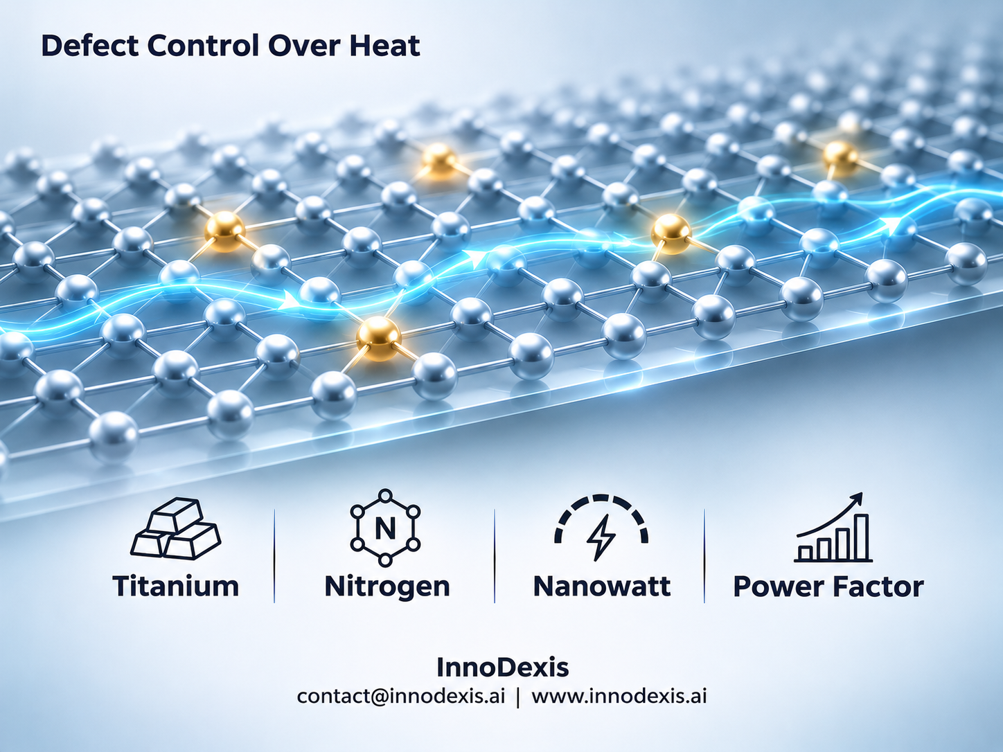
InnoDexis has published its latest Innovation Intelligence Report covering thermoelectric thin films for waste heat recovery, analyzing one innovation from Tohoku University in Japan, published on 29 October 2026. The report reveals that adding 4.6 to 9.3 atomic percent titanium to chromium nitride through room-temperature reactive sputtering raised the power factor 250-fold, by suppressing nitrogen vacancies and increasing electron mobility by approximately two orders of magnitude, and produced a prototype generator on a glass substrate that delivered 455.8 nW at a 96 K temperature difference, without high-temperature processing.
Key Findings
The power factor of the chromium nitride thin film rose 250-fold to 5.26 µW cm⁻¹ K⁻², compared with pure chromium nitride. The gain was achieved with room-temperature deposition, which removes the high-temperature processing that high-performance thermoelectric films have normally required.
Titanium works by suppressing nitrogen vacancies. Its higher affinity for nitrogen than chromium limits vacancy defects during sputtering, which raises electron mobility by approximately two orders of magnitude while reducing carrier concentration. This overcomes the usual trade-off between electrical conductivity and the Seebeck coefficient in room-temperature chromium nitride films.
A prototype thermoelectric generator on a glass substrate delivered a maximum power of 455.8 nW at a temperature difference of 96 K, equal to a power density of 38.0 mW cm⁻² normalized by thin-film cross-sectional area. This is comparable to existing high-performance materials that need high-temperature processing, although the absolute output remains in the nanowatt range.
The process depends on tight control of composition. Titanium content between 4.6 and 9.3 atomic percent produced the results, and keeping the doping precise during large-area sputtering is the main manufacturing requirement. The method uses standard reactive sputtering, which supports mass manufacturing.
The innovation is at laboratory prototype stage, with low commercial readiness. A period of 3 to 5 years is expected for specialized microdevice or flexible electronics applications, pending integration studies, and no regulatory approval requirement is apparent.
Strategic Insight and Trend Analysis
The dominant trend in this research is the substitution of defect control for heat treatment as the route to thermoelectric performance. Conventional chromium nitride films suffer high defect rates and poor mobility. Titanium doping controls those defects at room temperature, so the performance gain comes from the composition of the film rather than from an annealing step.
This matters because processing temperature has limited where thermoelectric films can be used. Room-temperature deposition lets high-density waste-heat-harvesting material be deposited directly onto heat-sensitive substrates and delicate microdevices. If it scales, the approach could move thermoelectrics into low-cost consumer electronics, wearables and other heat-sensitive systems, and could displace high-temperature processed materials in small-scale and flexible applications where thermal processing previously prevented integration. Yi Shuang, Assistant Professor at Tohoku University, describes the approach as a way to expand thermoelectric applications and recover energy that would otherwise be lost as heat.
The limits are specific. Output is in the nanowatt to microwatt range, which creates market adoption hurdles, and competing micro-power options such as thin-film batteries, micro-photovoltaics and piezoelectric harvesters are already available. The titanium window of 4.6 to 9.3 atomic percent is narrow, and the prototype was demonstrated on glass, with performance on flexible polymer substrates still to be shown.
The commercial question is therefore whether a process advantage in manufacturing can be turned into a product advantage, given low absolute power and the cost of integrating thin-film harvesters relative to the power they generate.
Global and Industry Implications
For corporates and R&D teams, electronics manufacturing and materials companies can adopt standard reactive sputtering pipelines to deposit thermoelectric coatings onto flexible substrates and microdevices. Identified uses include on-chip microdevice energy recycling and wearable self-powered sensors, and tight control of titanium concentration across large areas is the key process requirement.
For investors and capital allocators, the method is an enabler to monitor for low-cost, flexible thermoelectric components that avoid heat-treatment bottlenecks in microdevice assembly. The balance is clear: commercial readiness is low, a 3 to 5 year period is expected, and the cost of integrating harvesters is high relative to nanowatt-scale output. The narrow processing window and the scaling of sputter production for industrial energy-harvesting modules remain open technical risks.
For policymakers and national innovation bodies, the work points to waste heat recovery in electronic devices, factories and vehicles as the wider application space. No regulatory approval requirement is apparent at this stage, so the priorities are integration studies, long-term stability testing and the manufacturing scale-up that determine whether laboratory results reach industry.
InnoDexis Statement
“Replacing high-temperature processing with room-temperature defect control opens heat-sensitive substrates to thermoelectric films, and holding titanium within a narrow window at scale now decides whether nanowatt-scale output finds a market,” noted InnoDexis in its latest intelligence report.
Conclusion
The next milestones to watch are evaluation of long-term thermal stability and power maintenance under continuous heat gradients, demonstration of prototype performance on flexible polymer substrates, and optimization of deposition rates and film uniformity over large surface areas. Testing across broader operating temperature ranges will show how far the results carry beyond the laboratory. InnoDexis will continue to track thermoelectric thin films, waste heat recovery and flexible electronics energy harvesting as this field develops. The complete Thermoelectric Thin Film Innovation Intelligence Report is available to InnoDexis subscribers and enterprise clients.
About InnoDexis
InnoDexis is a real-time innovation intelligence platform connecting scientific discovery to commercial opportunity. Powered by InnoGraph, its proprietary innovation knowledge graph, the platform maps technologies across the entire lifecycle, from early-stage research (TRL 1) to market deployment (TRL 9), connecting researchers, institutions, startups, companies, products and emerging opportunities.
Covering 40+ specialised industry segments and 360 technology areas, InnoDexis delivers innovation tracking, research discovery, product and startup intelligence, investment insights, and AI-powered reports. Its mission is to bridge the gap between scientific discovery and real-world impact.
InnoDexis — From Lab to Market: Real-Time Innovation Intelligence.