Room-Temperature Metal-Organic Framework Etching With Ionic Liquids Reaches 130–300 nm Lines, No Cryogenic Cooling, at Tokyo University of Science
Tokyo University of Science researchers filled MOF pores with imidazolium-based ionic liquids, raising hardness and thermal stability so a focused gallium ion beam could etch Cu3BTC2 at room temperature with substantially less structural damage.
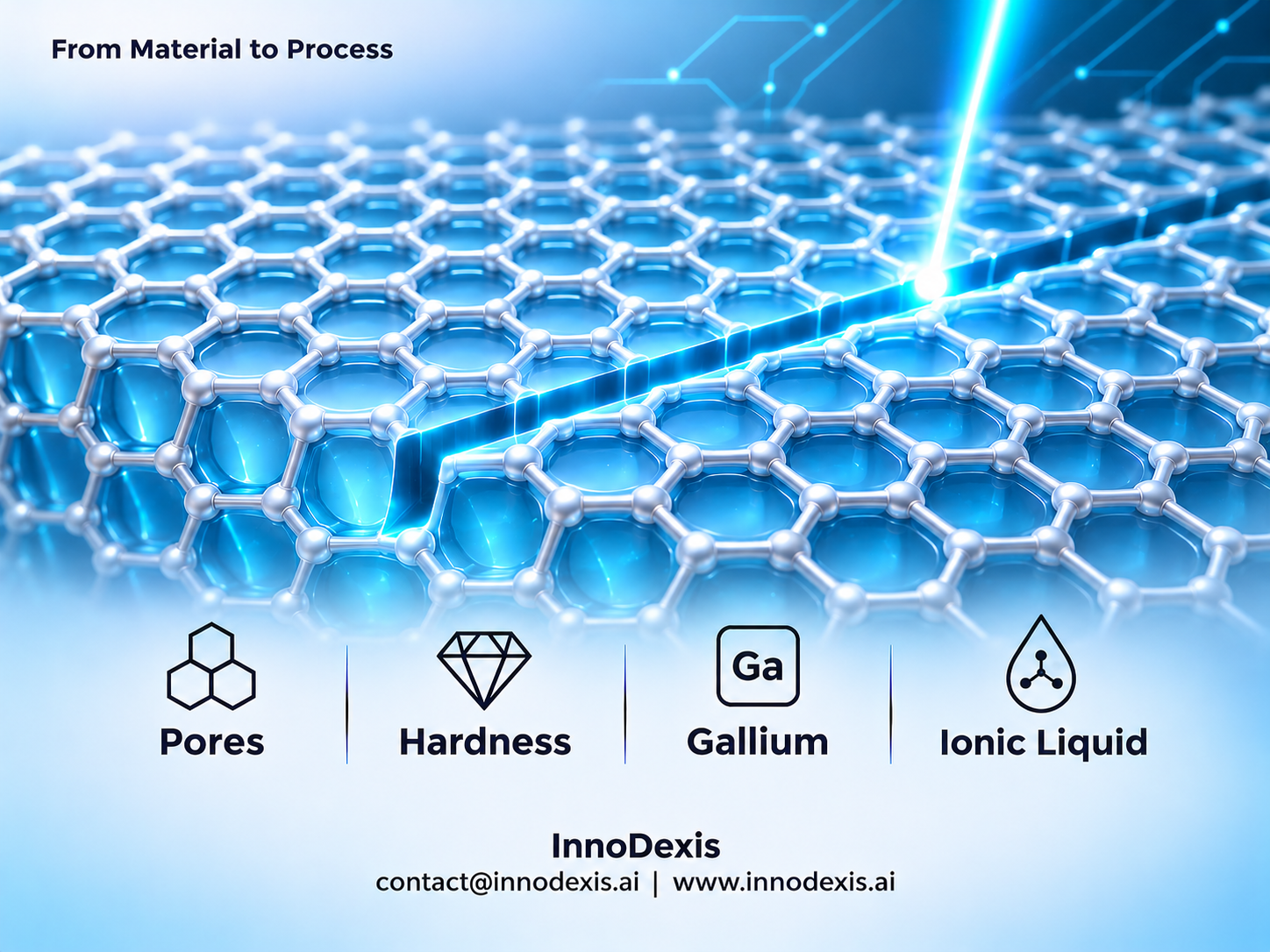
InnoDexis has published its latest Innovation Intelligence Report covering microfabrication of fragile metal-organic frameworks, analyzing one innovation from Japan, published on 10 November 2026. The report reveals that, in a proof-of-concept demonstration, Tokyo University of Science researchers developed the first room-temperature dry etching method for metal-organic frameworks using ionic liquid protection, filling 50–60% of the pore volume with imidazolium-based ionic liquids so that focused ion beam etching produced lines 130–300 nm wide without cryogenic cooling and with substantially less microstructural damage.
Key Findings
The method is the first room-temperature dry etching approach for metal-organic frameworks that uses ionic liquid protection. Cryogenic etching was previously the only known way to physically etch these materials while preserving their delicate structures, so removing the need for liquid nitrogen cooling equipment takes out a major barrier to microfabrication.
Ionic liquids filled 50–60% of the pore volume of the frameworks. The filled material showed increased hardness, improved mechanical stability and decomposition at higher temperatures, and the etched structures showed substantially less apparent microstructural damage from the focused gallium ion beam. The filling also helps dissipate thermal and electrical charge during beam exposure.
Etching produced lines 130–300 nm wide in Cu3BTC2. Demonstration patterns included a pillar, a 5 × 5 µm2 square and an etched Chinese character, which together show that fragile frameworks can be patterned at the nanometre scale at room temperature.
More than 100,000 MOFs are known, which defines the scale of the opportunity for the method. The demonstration so far is primarily on copper-based Cu3BTC2, so extension to other frameworks remains to be shown, and the method adds a step to infiltrate the pores with ionic liquid.
The work is at proof-of-concept stage, with commercial readiness rated low to medium. Pilot integration into specialised sensor or electronic device manufacturing is estimated at 3 to 5 years, and scalability potential is rated high because ionic liquids and standard focused ion beam equipment are widely available.
Strategic Insight and Trend Analysis
The dominant trend in this research is a shift in the barrier to using metal-organic frameworks in devices, from the material to the process. The functional properties of MOFs are not in question. What has limited their use in electronics is that the structures are too fragile to survive conventional patterning, and cryogenic etching, the only known workaround, requires complex liquid nitrogen cooling.
The Tokyo University of Science approach changes the equation by protecting the framework rather than cooling it. Filling the pores with ionic liquid raises hardness and thermal stability, and the same dissipation of thermal and electrical charge that protects the material allows room-temperature etching with standard focused ion beam equipment. If it holds up, the method could displace specialised cryogenic etching protocols in semiconductor and MEMS fabrication for fragile porous materials. Kentaro Kinoshita describes the potential as a foundational technology that connects the functions of MOFs with practical devices.
The open questions are specific. Ionic liquid infiltration must not permanently alter the porous properties that downstream applications need, so post-etching extraction processes are required where open porosity is essential. Compatibility with other MOF classes and pore geometries is untested, and market adoption depends on compatibility with standard semiconductor fabrication flows. Alternative non-destructive patterning methods and damage-resistant MOF formulations are the main competing routes. The practical question is whether the infiltration and removal steps can be run at industrial volumes, which the research identifies as needing engineering optimization.
Global and Industry Implications
For corporates and R&D teams in semiconductors, MEMS and sensors, the method bypasses dedicated cryogenic cooling hardware and needs conventional room-temperature dry etching toolsets adapted with a pre-etching infiltration step. Applications named include high-sensitivity sensors, separation and analysis devices, catalytic devices, resistive switching memory, integrated chemical separation chips and on-chip micro-catalytic reactors. Integration of etched MOF structures into functional electronic and micro-sensor prototypes is the next step these teams will need.
For investors and capital allocators, the profile is early and technical. The work is at proof-of-concept stage with low-to-medium commercial readiness and a 3 to 5 year horizon to pilot integration. Scalability potential is high, although liquid infiltration and removal at industrial volumes will need engineering optimization, and no regulatory approval is apparent. Alternative non-destructive patterning methods and damage-resistant MOF formulations are the identified threats.
For policymakers and national innovation bodies, the research was supported by a JSPS KAKENHI grant and involved the University of Tokyo, Doshisha University, the University of Melbourne and Tokyo University of Science. It illustrates how research grant funding can address a manufacturing barrier in advanced materials that sits between laboratory discovery and device use.
InnoDexis Statement
“Replacing cryogenic cooling with a pore-filling step moves the barrier to using metal-organic frameworks in devices from the material to the process, and compatibility with standard semiconductor fabrication flows will decide its reach,” noted InnoDexis in its latest intelligence report.
Conclusion
The next milestones to watch are validation of the method on MOF classes beyond copper-based frameworks, post-etching processes that clear ionic liquids where open porosity is needed, and integration of etched MOF structures into functional electronic and micro-sensor prototypes. Optimizing ionic liquid selection for different pore geometries is a further open task. Pilot integration is estimated at 3 to 5 years. InnoDexis will continue to track metal-organic framework microfabrication, ambient-condition semiconductor processing and functional nanomaterials as this field develops. The complete Metal-Organic Framework Room-Temperature Etching Innovation Intelligence Report is available to InnoDexis subscribers and enterprise clients.
About InnoDexis
InnoDexis is a real-time innovation intelligence platform connecting scientific discovery to commercial opportunity. Powered by InnoGraph, its proprietary innovation knowledge graph, the platform maps technologies across the entire lifecycle, from early-stage research (TRL 1) to market deployment (TRL 9), connecting researchers, institutions, startups, companies, products and emerging opportunities.
Covering 40+ specialised industry segments and 360 technology areas, InnoDexis delivers innovation tracking, research discovery, product and startup intelligence, investment insights, and AI-powered reports. Its mission is to bridge the gap between scientific discovery and real-world impact.
InnoDexis — From Lab to Market: Real-Time Innovation Intelligence.