Reconfigurability Emerges as the Competitive Axis Across 81 Research Announcements as US Defence Agencies Fund Nearly One in Five Records and Only Two Technologies Are Demonstrated Outside a Laboratory
A latest-report analysis of 81 photonic and metamaterial engineering research records across 67 institutions and 15 countries finds that design throughput has collapsed from months to milliseconds while fabrication capability has not moved, creating the widest structural gap in the field.
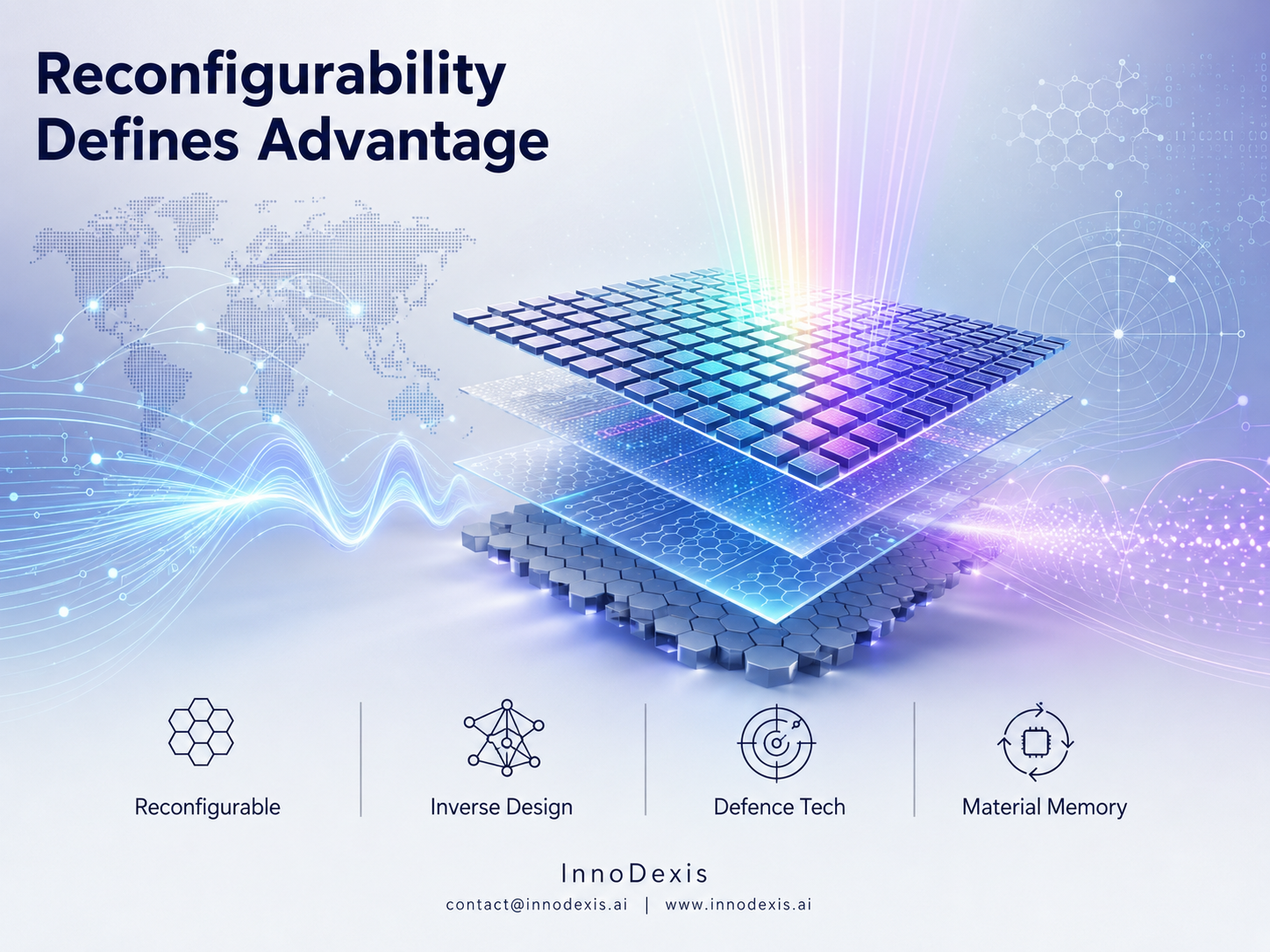
InnoDexis has published its latest Innovation Intelligence Report covering photonic and metamaterial engineering, analyzing 81 research announcements across 67 institutions and 15 countries. The report reveals that reconfigurability — the ability of a structured surface to change its behaviour on command — has become the field's primary competitive axis, that 74% of announcements carry a quantified result while only five name a path to fabrication, and that United States defence agencies appear as funders in eight announcements — nearly one in five of all funded records — concentrated in terahertz sensing, radar countermeasures, and reconfigurable infrared surfaces.
Key Findings
The corpus divides into four domains with metasurfaces and flat optics at the centre. Of 81 announcements, 40 concern metasurfaces and flat optics directly, 16 extend the same structuring logic to light generation and detection, 13 to mechanical deformation, and 12 to heat transport. No institution appears more than three times across 67 distinct institutions, confirming a highly fragmented field with no dominant centre. Three quarters of announcements name more than one institution, with a mean of 2.8 affiliations and approximately half describing cross-border collaboration explicitly.
Reconfigurability is the dominant competitive axis and every announced result addresses control rather than static performance. KAIST demonstrated stable performance across more than 16,700 switching cycles on an individually addressable mid-infrared metasurface — approximately 13 times prior endurance benchmarks. MIT achieved two-dimensional pixel-level control of phase-change metasurfaces. University of Stuttgart converted a metasurface into a programmable platform. The gap between these demonstrations and commercial utility is several orders of magnitude in pixel count and cycle endurance, and no announcement in the corpus claims to have closed it.
Design cost has collapsed and that redistribution of advantage is the most strategically consequential pattern in the corpus. Penn State reports metasurface design time falling from months to milliseconds through neural inverse design of free-form metasurfaces. Tsinghua reports a diffusion model that removes iterative optimisation entirely, with designs described as fabrication-ready. The asymmetry this creates is structural: inverse design can now produce a metasurface layout in milliseconds and nothing in the corpus can fabricate one at comparable speed or scale. When simulation stops being the bottleneck the moat moves to fabrication capability and to whoever holds the training data.
Three foundational tradeoffs have been broken rather than negotiated within the corpus window. Harvard demonstrated that low-refractive-index silica materials can produce high-performance metasurfaces, directly contradicting an assumption the field was built on — and carrying commercial significance because silica is cheap and CMOS-compatible where high-index alternatives are not. CUNY achieved approximately 100 times third-harmonic efficiency improvement over comparable devices, breaking the efficiency-versus-control tradeoff. Osaka University exceeded the theoretical 50% ceiling for circularly polarised light conversion, reaching 68% linear-to-circular efficiency with polarisation control built into the device rather than added downstream.
Two independent domains arrived at processor-free material memory within the same reporting window. Osaka Metropolitan University built a thermal device — using a magneto-optical and GST combination — that switches the direction of heat radiation and retains its state without power. The University of Amsterdam built a metamaterial that learns and retains multiple shape-changing strategies with no central processor, demonstrating object grasping and locomotion. Different physics, different continents, the same architectural idea: put the state in the material rather than in a controller.
The fabrication gap is the field's defining constraint and the researchers are unusually candid about it. Of 81 announcements, 64 carry laboratory proof of concept and 35 describe a working prototype, while only five name a specific path to fabrication and only two describe anything demonstrated outside a laboratory — Seoul National University's transparent radiative cooling film tested on vehicle glazing, reducing cabin temperature by up to 6.1 degrees Celsius and cutting cooling energy consumption by more than 20% in road tests, and an urban heat-adaptation social-science study. Durability and long-term stability is named as a barrier by 22% of the corpus — the most common self-reported constraint by a wide margin — with large-area nanofabrication and cost each appearing at 10%.
Strategic Insight and Trend Analysis
The most consequential structural finding of the photonic and metamaterial engineering report is the widening asymmetry between design throughput and fabrication throughput. These two capabilities have historically moved together because both required human expertise. Machine-learned inverse design has decoupled them: one side is improving at software speed while the other remains constrained by physical process development. The first organisation to resolve the fabrication side will inherit a backlog of validated designs that nobody else can yet build — a structural advantage that does not require any further scientific advance to realise.
The defence funding signal adds a second structural layer that the announcement framing obscures. Eight records naming US Air Force, Department of Defense, Defense Threat Reduction Agency, and Department of Energy national-security contracts as funders represent nearly one in five of all funded records in the corpus. The technologies attracting that funding are consistent — terahertz sensing and imaging, radar countermeasures, reconfigurable mid-infrared surfaces framed as space sensors, and neutral-atom quantum arrays — confirming that what reads as a civilian optics field has a sensing and counter-sensing funding structure beneath it. Several announcements name both NSF and defence sources simultaneously, indicating that the field is not being divided into civilian and defence tracks but is being jointly funded across both.
Germany is the national result worth most attention. Twelve announcements spread across all four domains, and uniquely across the 15-country field, Germany is the only country contributing programme-level infrastructure — the Laser Fusion Hub naming thirteen participants mixing companies, research infrastructures, universities, and government, and the META-ACTIVE graduate school entering its second funding phase — rather than results alone. On the evidence of this corpus Germany is building durable capacity while others publish discrete output.
Global and Industry Implications
For corporates and R&D teams, the five records naming a fabrication pathway are the actionable commercial entry points in the corpus. POSTECH's dual-function single-layer dielectric metasurface, ETH Zurich's vibration-guiding metamaterial using conventional silicon wafer fabrication, Tsinghua's fabrication-ready AI-generated photonics designs, the Chinese Nuclear Chemical Society's Mg₂Al₄Si₅O₁₈ cooling ceramic with synthesis and coating described as suitable for mass production, and A*STAR's 12-inch DUV fabrication route each represent a point where the distance between demonstrated result and manufacturable product is shorter than anywhere else in the corpus. The thermal materials domain carries the highest density of quantified results in the report and the only mass-production route claim outside the metasurface domain, identifying it as the commercial entry tier for organisations whose supply chains involve cooling, cryogenics, or energy efficiency at industrial scale.
For investors and capital allocators, the processor-free material memory convergence across Osaka Metropolitan and Amsterdam represents the class of result that becomes strategically consequential if a third independent instance appears — the report explicitly identifies this as the signal that would make processor-free state retention the defining trend of the period rather than a coincidence of two results. The NIMS rare-earth-free cryogenic regenerator material reaching practical performance at approximately 4 Kelvin, matching holmium-based conventional materials, and Darmstadt's magnetocaloric materials with reversible adiabatic temperature change more than doubled from 3.8 to 8 degrees Celsius each address supply-chain exposure directly — a claim no other result category in the corpus makes — identifying the thermal and cooling materials domain as the highest near-term commercial relevance tier for investors concerned with critical materials dependencies.
For policymakers and national innovation bodies, the cross-border funding structure documented across the corpus — Korean results naming both Korean and US Air Force sources, Harbin drawing simultaneous Chinese and Russian state funding, and Harvard combining NSF and Swiss National Science Foundation support — confirms that research funding in this field crosses geopolitical boundaries more readily than technology policy frameworks currently anticipate. The Korea National Research Foundation and Ministry of Science appearing nine times against seven Korean announcements — effectively 100% state co-funding of all Korean work — and the German programme-infrastructure model each represent distinct national strategies for developing durable capacity in a field where individual results are highly fragmented and no single institution dominates. The watchlist item most directly addressable through policy is Harvard's low-index silica metasurface result: if independently replicated, it would eliminate the exotic high-index material requirement that currently constrains CMOS-compatible manufacturing of metasurface devices, and national semiconductor fabrication investment programmes should monitor replication attempts before committing to high-index material supply-chain development.
InnoDexis Statement
"The photonic and metamaterial engineering field can now design a metasurface in milliseconds and cannot manufacture one at scale — and whoever closes that gap first will inherit a backlog of validated designs that the rest of the field cannot yet build," noted InnoDexis in its latest intelligence report.
Conclusion
The photonic and metamaterial engineering report establishes that reconfigurability has become the field's competitive axis, that the design-fabrication asymmetry opened by machine-learned inverse design is the widest structural gap in the corpus, and that a defence funding structure beneath a civilian announcement surface funds nearly one in five records in identifiable sensing and counter-sensing applications. Across 81 research announcements from 67 institutions and 15 countries, the evidence confirms processor-free material memory converging independently across thermal and mechanical domains, five fabrication pathways as the corpus's rarest and most commercially proximate finding, and Germany as the only country building programme-level research infrastructure rather than reporting discrete results. As KAIST's cycle endurance and array sizes are tracked against commercial thresholds, Harvard's low-index silica result is monitored for independent replication, Seoul National University's cooling film advances toward automotive and glazing manufacturer engagement, and the thermal materials domain is tested for scale-up beyond laboratory regenerators, the Photonic and Metamaterial Engineering framework will provide the most structurally precise early-signal intelligence on this field the InnoDexis platform has yet produced. The complete Photonic and Metamaterial Engineering Latest Report is available to InnoDexis subscribers and enterprise clients.
About InnoDexis
InnoDexis is a global Innovation Intelligence platform that tracks, analyzes, and interprets breakthrough innovations, prototypes, and emerging technologies across industries and countries. Its intelligence helps corporates, investors, and policymakers understand the true structure and direction of global innovation. Learn more at innodexis.ai.