Harvard, UT Austin, and UC Irvine Achieve 1,000x Nonlinear Optical Efficiency Gain on Chip-Scale Semiconductor Platform
By jointly engineering quantum well energy levels and metasurface field symmetry in a single chip-scale device, researchers have boosted nonlinear optical frequency conversion efficiency by three orders of magnitude over unpatterned wafers.
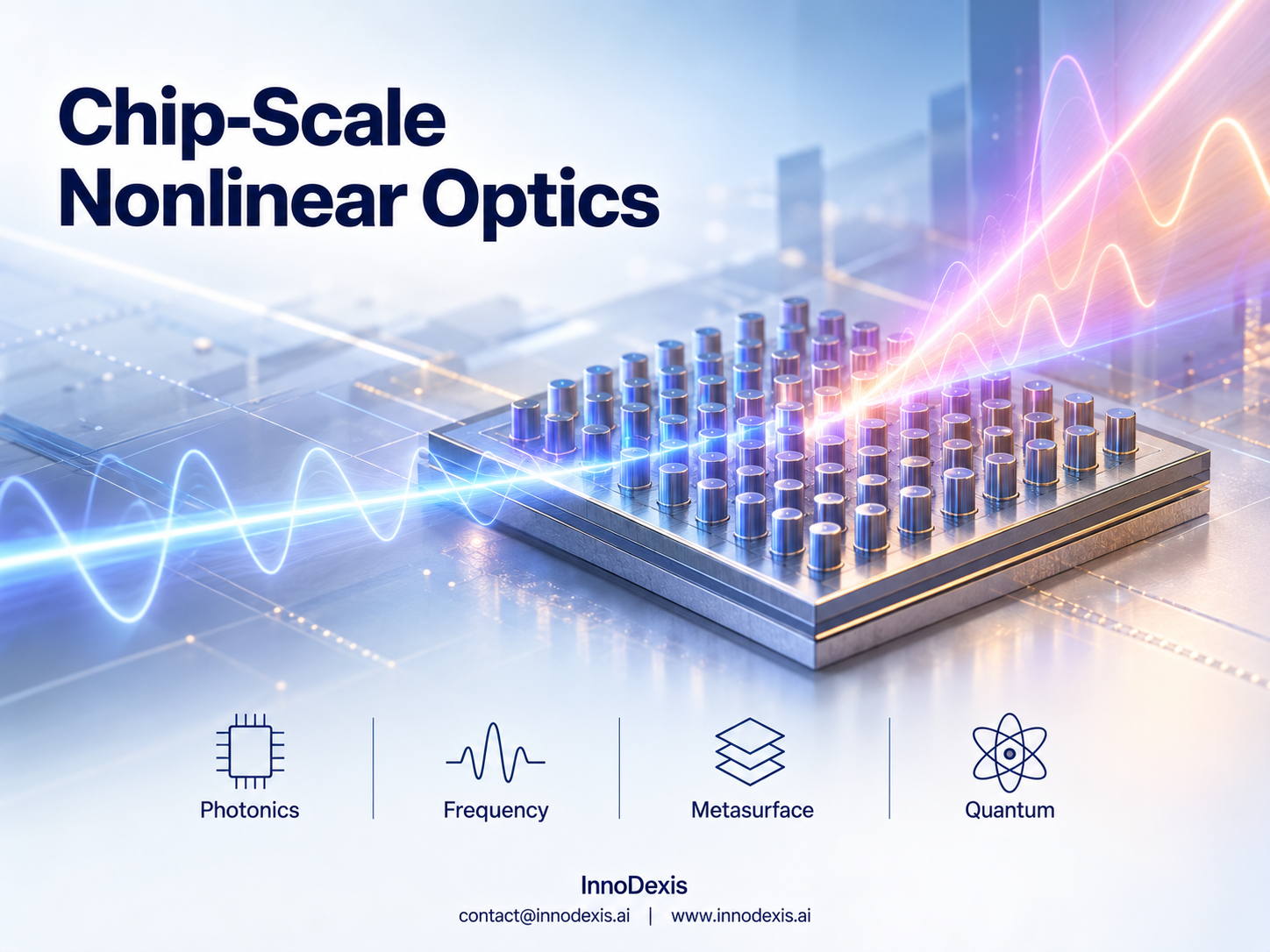
InnoDexis has published its latest Innovation Intelligence Report covering chip-scale nonlinear optics and photonic integration, analyzing a high-significance innovation from the United States. The report reveals that researchers at Harvard SEAS, the University of Texas at Austin, and the University of California Irvine have combined multi-quantum well semiconductors with metasurface nanopillar arrays to achieve a 1,000x improvement in nonlinear optical frequency conversion efficiency — overcoming a long-standing barrier that has prevented nonlinear optical components from reaching chip scale and enabling a new class of compact photonic and quantum devices compatible with standard semiconductor manufacturing processes.
Key Findings
Nonlinear optical conversion efficiency was boosted by three orders of magnitude — 1,000x — over unpatterned wafers through the joint engineering of quantum well energy levels and metasurface field symmetry within a single device. This result was produced by combining multi-quantum well semiconductors with metasurface nanopillar arrays, an approach that tailors both material and electromagnetic field dynamics simultaneously rather than relying on fixed bulk crystal structures with predetermined optical properties.
The platform is compatible with standard GaAs and AlGaAs compound semiconductor materials and planar nanofabrication processes. This compatibility is a defining characteristic of the innovation's strategic significance: it means the approach can enter existing semiconductor manufacturing lines without requiring new materials ecosystems or fabrication infrastructure, substantially lowering the barrier to industrial adoption.
The nonlinear response achieved is larger than either the quantum well or the metasurface component could produce in isolation. This emergent performance gain — arising specifically from the joint engineering of quantum and electromagnetic properties in one device — establishes a design principle that goes beyond incremental improvement within either field individually.
A non-traditional electronic transition in the quantum wells was used to reach shorter near-infrared wavelengths. This methodological choice extends the accessible wavelength range of the platform and broadens the set of photonic and quantum applications the device can address, including frequency conversion at wavelengths relevant to quantum communication and atomic clock operation.
The platform enables a defined set of chip-scale device categories: frequency converters, entangled photon pair sources, and chip-scale atomic clocks. Each of these represents an application class where the transition from bulky nonlinear optical crystal components to chip-scale integration has been a persistent technical barrier — one this platform directly addresses through compatibility with planar nanofabrication.
Strategic Insight and Trend Analysis
The dominant trend this dataset signals is the convergence of quantum engineering and electromagnetic design into a single device architecture — a departure from the conventional approach of optimising each independently and then combining them at the system level. The 1,000x efficiency gain is the measurable outcome of this convergence, but the structural implication is broader: jointly engineering quantum and field responses within one chip-scale platform establishes a new design paradigm for nonlinear photonics.
Bulk nonlinear optical crystals have defined the architecture of photonic and quantum optical systems for decades, primarily because no chip-compatible alternative could match their nonlinear conversion performance. The persistence of this constraint has meant that entire device categories — quantum light sources, frequency converters, atomic clocks — have remained dependent on components that resist miniaturisation. The Harvard-UT Austin-UC Irvine platform removes the performance argument for retaining bulk crystal components in these application classes, at least at the frequency conversion efficiency level.
The compatibility with planar nanofabrication is the second strategic dimension. A 1,000x efficiency gain produced by a platform that requires entirely new manufacturing infrastructure would face a long adoption timeline regardless of its performance. Compatibility with existing GaAs and AlGaAs fabrication processes means the path from research demonstration to manufacturable device is defined by engineering development rather than infrastructure investment — a materially shorter transition.
Together, these two dimensions — a new design paradigm and a manufacturing-compatible implementation — suggest that this innovation is positioned not as a long-cycle basic science advance but as a near-to-medium-term platform for photonic and quantum device development across multiple application areas simultaneously.
Global and Industry Implications
For corporates and R&D teams in photonics, semiconductors, and quantum hardware, the platform's compatibility with standard GaAs and AlGaAs planar nanofabrication represents an immediately actionable signal. Organisations with existing compound semiconductor manufacturing capabilities are structurally positioned to evaluate integration of this approach into photonic integrated circuit development pipelines without requiring new materials or process infrastructure.
For investors and capital allocators, the innovation identifies a credible path toward chip-scale quantum communication hardware and compact atomic clock components — two application categories with growing strategic and commercial relevance. The platform's derivation from standard semiconductor materials reduces the manufacturing risk profile compared to quantum photonic approaches requiring exotic or non-standard fabrication environments, making it a more near-term investment-relevant signal within the quantum photonics landscape.
For policymakers and national innovation bodies, the research — conducted across three leading US research universities — illustrates the value of multi-institutional collaboration in producing platform-level photonic innovations. As quantum communication infrastructure becomes a national strategic priority across multiple governments, chip-scale nonlinear optical platforms compatible with existing semiconductor manufacturing represent a critical enabling technology layer warranting targeted research investment.
InnoDexis Statement
"The joint engineering of quantum well energy levels and metasurface field symmetry in a single chip-scale device reframes the nonlinear optics design paradigm — moving the field from fixed bulk crystal architectures toward tunable, semiconductor-compatible platforms with direct implications for quantum and photonic integration," noted InnoDexis in its latest intelligence report.
Conclusion
As quantum communication, photonic integration, and compact timing technologies move toward semiconductor chip-scale implementation, the availability of a nonlinear optical platform achieving 1,000x efficiency gains within standard fabrication processes marks a structural shift in what chip-scale photonic devices can deliver. The transition from bulk crystal components to jointly engineered quantum-metasurface architectures will be a development to monitor closely across photonics, quantum hardware, and semiconductor manufacturing. InnoDexis will continue tracking advances in chip-scale nonlinear optics, metasurface engineering, and quantum photonic device development. The complete Chip-Scale Nonlinear Optics Innovation Intelligence Report is available to InnoDexis subscribers and enterprise clients.
About InnoDexis
InnoDexis is a global Innovation Intelligence platform that tracks, analyzes, and interprets breakthrough innovations, prototypes, and emerging technologies across industries and countries. Its intelligence helps corporates, investors, and policymakers understand the true structure and direction of global innovation. Learn more at innodexis.ai.
[HASHTAGS]
#InnoDexis #NonlinearOptics #Nanophotonics #QuantumPhotonics #Metasurfaces #PhotonicIntegratedCircuits #QuantumCommunication #Semiconductors #ChipScaleOptics #USAInnovation